
- TSMC has said that its N3 process wafer capacity could remain tight for multiple years, with companies across the tech sector confirming this constraint.
- The largest AI chip designers, including Nvidia, Google, and others, are converging their flagship platforms on N3 simultaneously as sales are expected to soar.
- Amid TSMC’s wafer constraints, Intel is betting on its 18A and 14A processes to win over AI customers. This provides Intel an opening to generate significant external foundry sales, but only if can execute.
Nvidia is moving its next-generation Rubin GPUs from 4nm to 3nm, yet Google’s latest TPUs are already on N3 and are expected to remain there. Meanwhile, a growing number of AI CPUs from Nvidia, Amazon, Microsoft, and Arm are converging on the same node.
TSMC has already reached its planned capacity for N3, and announced another expansion in April 2026. Management has stated that 3nm capacity could remain tight for several years, while semiconductor companies are echoing concerns around 3nm constraints.
This creates an opportunity for Intel given that it’s Arizona capacity is coming online whereas TSMC’s new fabs largely will not arrive until late 2027. However, available capacity is not the same thing as customer demand. Intel must still convince major chip designers that 18A and eventually 14A can meet their performance and yield requirements. This means the advanced node opportunity is more speculative than the packaging opportunity – but also much larger if Intel can convert TSMC’s bottleneck into design wins.
For more information on Intel’s advanced packaging opportunity that explores how customers for TSMC CoWoS could design their chips to be compatible with EMIB-T packaging, read “Intel vs TSMC: How CoWoS Packaging Constraints Could Create an Opportunity for Intel Foundry“
Advanced Nodes Drive 77% of TSMC’s Wafer Revenue
Advanced node wafers have been a huge growth driver for TSMC. The company is guiding for a mid-to-high 50% AI growth CAGR from 2024-2029. TSMC did not update the figure in Q2, but said its expectations have become “stronger and stronger and stronger” since its last update. Last quarter, 77% of wafer revenue came from advanced node technologies, with 66% of revenue coming from its High-Performance Computing (HPC) platform.
Meanwhile, Intel has yet to participate meaningfully in advanced node wafer sales, with its external foundry revenue being just $293 million in Q2. TSMC’s total Q2 sales of $40.2 billion were 137X higher, demonstrating the huge size of the external foundry market that Intel is looking to penetrate.
TSMC’s N3 Constraints Echoed Across the Industry
Advanced packaging is a prevalent constraint on TSMC, but advanced node wafer capacity is tight as well. TSMC noted in July 2025 that its N3 capacity was “very tight” and that this will be “continued for a couple of years.”
Notably, this imbalance is being corroborated by players across the AI and semiconductor industry.
- Apple CEO Tim Cook, January 2026: “it’s the advanced nodes that we — like 3-nanometer to be specific, where our SoCs or the latest SoCs are produced on as to what is gating the Q2 supply”
- Microchip CEO Steve Sanghi, May 2026: “the major tightness would be really on the bleeding edge like 3-nanometer.”
- AMD VP Matt Ramsay, June 2026: “I think one thing that I’ve noticed is supply is tight. 3-nanometer is tight.”
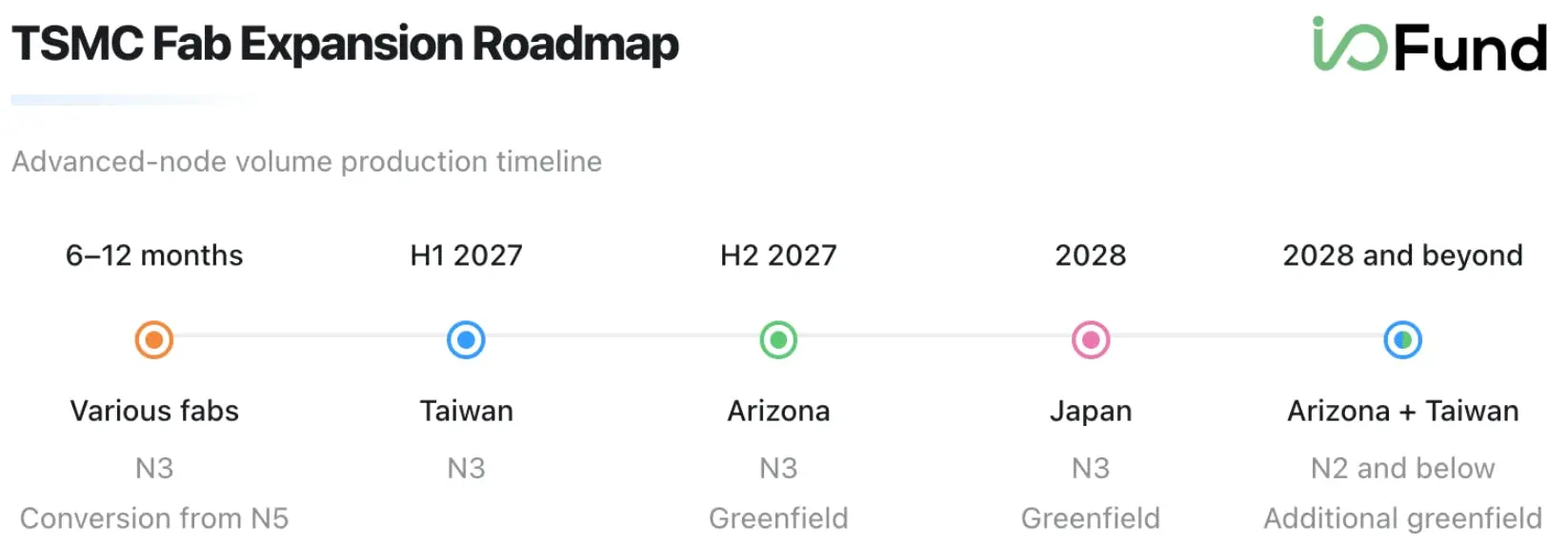
- Credo CEO Bill Brennan, June 2026: “So you’re talking about a potential real crunch in 3-nanometer capacity. It’s been discussed at an industry level for several months now. And there’s an indicator from TSMC, they’re bringing on huge capacity in Taiwan and Japan and Arizona, but that’s really a ’28 kind of time frame.”
In April 2026, TSMC announced that it would add additional N3 capacity. This is unusual, as N3 had already hit its target capacity level, and the company does not typically increase capacity at a certain node after this point. However, to support a “robust multi-year pipeline of demand” TSMC will increase its capex investment in N3 capacity, which is used across smartphone, HPC, AI and other end markets. This shift signals an unexpectedly high degree of demand and a supply imbalance for N3.
Nvidia, Google, and Others Are Converging on N3
The world’s largest AI chip designers are converging on the same node, at the same time.
Nvidia’s current generation Blackwell systems are built on TSMC’s N4 process, but its next generation Rubin systems will be built on N3. To grasp the size of the Rubin ramp, consider that Wolfe Research expects Nvidia to sell 55,000 Rubin racks and 15,000 Rubin Ultra racks in 2027. Meanwhile, the current estimates place the price of a Rubin rack at $7.8 million. Together, these estimates imply revenue of over $550 billion for these systems alone, as Rubin Ultra would be priced higher. That is more than double Nvidia’s last 12 months revenue of $253 billion. This ramp could place substantial pressure on TSMC’s N3 capacity.
Additionally, Google’s TPU Ironwood v7 used N3 and the TPU v8 will remain on N3. The TPU ramp is also expected to be very large as we move into 2027. Wolfe estimates that TPU shipments will rise from approximately 3.3 million in 2026 to 5.1 million in 2027, a nearly 55% increase. This aligns with Morgan Stanley’s estimate for 5 million TPU shipments in 2027, demonstrating the strong growth expectations for Google’s custom silicon that will further pressure N3 capacity.
Several CPUs, including Arm’s AGI CPU, Amazon’s Gravitron5, Microsoft’s Cobalt 200, and Nvidia’s Vera will all use N3. While Nvidia GPUs and Google’s TPUs will take up the largest shares of N3 capacity, CPU demand is also important to take notice of.
CPU N3 demand comes at a time when the ratio of GPU to CPU content in AI data centers is expected to shift from between 1:4 and 1:8 to between 1:1 to 1:2. This is causing expectations for CPU sales growth to see dramatic upward revisions. Notably, Nvidia has visibility into generating $20 billion in CPU sales in 2026, significantly higher than AMD’s current CPU run-rate. Thus, rising CPU demand could place meaningful pressure on N3 capacity as well.
To learn more about why Agentic AI is causing CPU growth expectations to soar, read our June analysis: AMD, Nvidia, Arm, Intel: Inside the $120 Billion CPU Gold Rush
How TSMC and Intel Are Expanding Advanced Node Capacity
TSMC and Intel are both taking action to expand advanced node production capacity in light of this. One of the primary actions that TSMC is taking is converting its higher node capacity into lower node capacity, particularly from N5 to N3. This is possible as the company says that N7, N5, N3, and even N2, share around 85% to 90% of common tools. These conversions are more cost efficient and expedient ways to add capacity in comparison to greenfield fab expansions, but they are still far from immediate, taking between 6 to 12 months.
Intel is also expanding and enhancing its Leixlip campus in Ireland, recently announcing a €5 billion ($5.7 billion) investment. Intel says that this investment will go toward upgrading existing facilities, and installing leading-edge manufacturing equipment. The investment will scale capacity for its Xeon processors, built on its Intel 3 process. Intel also said it will “increase what we can deliver to Intel Foundry customers”, although did not outline any actual allocation to third parties. This flexibility provides a pathway for Intel to scale external foundry sales at Leixlip on its advanced Intel 3 process should it attract demand.
However, 18A and 14A are the company’s most advanced nodes, and the ones it is banking on to attract AI accelerator demand.
Most New TSMC Capacity Will Not Arrive Until Late 2027 or Beyond
TSMC’s conversion strategy provides a more immediate path to increase capacity at nodes like N3. However, this strategy is still bounded by the need to provide supply for higher process nodes. In turn, TSMC is also aggressively building new fabs across Taiwan, Arizona and Japan, with several capacity additions set for H1 2027 and beyond.