
This article was originally published on Forbes on May 30, 2024,03:26pm EDT
Taiwan Semiconductor (TSMC) is the supplier for major design companies, such as Apple, Nvidia, AMD, Arm, Qualcomm, Broadcom, MediaTek and Marvell. TSMC is a foundry that manufactures the world’s most advanced chips, designated by node size. The most advanced node in production today is the 3nm and is primarily used by Apple in iPhones and MacBooks. The 5nm/4nm is used by Nvidia and others for AI accelerators, with high-performance computing quickly moving to 3nm and even 2nm.
Taiwan Semiconductor reported earnings on April 18th. The company topped analyst estimates and its internal guide with revenue growth of 12.9% YoY growth for US$18.9 billion. EPS beat by 4.5% at $1.38 reported compared to $1.32 expected.
Advanced node revenue continues to remain strong, though 3nm revenue dipped sequentially. Per the opening remarks: “3-nanometer process technology contributed 9% of wafer revenue in the first quarter.” This is down from 15% last quarter. The decline is temporary with Trend Force expecting 3nm production capacity utilization to be up 80% by year end. This quarter, revenue from 5nm and 7nm both expanded 2 points.
Despite warning of a slowdown in the broader semiconductor industry this year, TSMC’s April sales surged 60% YoY and 21% MoM. This marks a positive start to the 20-percentage point acceleration to 33% revenue growth that analysts expect as soon as the September quarter.
Sign up for I/O Fund’s free newsletter with gains of up to 485% – Click here
Background on Advanced Nodes: 5nm, 3nm and upcoming 2nm
Currently, AI accelerators use TSMC’s 5nm process. Nvidia’s Hopper and Blackwell are built with a N4X process that is tailored for high-performance computer applications. This is a customized variant called “4N” that Nvidia uses, yet TSMC recognizes this as 5nm revenue in their earnings report. AI accelerators are expected to quickly move to smaller nodes to help lower power consumption. TSMC’s 3nm process is more energy efficient, and energy efficiency will improve further with the 2nm process.
3nm (N3) and 2nm (N2) technology:
The 3nm process is currently the most advanced semiconductor technology, representing a full node advance from the 5nm generation. At the foundry level, the 3nm process offers 15% better performance than the 5nm process when power level and transistors are equal. TSMC also states the 3nm process can lower power consumption by as much as 30%. The die sizes are also an estimated 42% smaller than the 5nm.
In 2023, TSMC made 3nm chips for Apple’s iPhone 15 Pro, iPhone 15 Pro Max and MacBook’s M3 chips. In 2024, TSMC will expand its 3nm customers to include AMD and Intel. What is interesting is that Nvidia is not using the 3nm node in 2024, despite industry-wide expectations Blackwell would feature the most advanced node. Instead, Blackwell is relying on architecture for its advancement leap from the Hopper architecture.
TSMC offers enhanced 3nm processes, such as the N3E, N3P and N3X, which allows a company like Apple to customize the 3nm chips differently than those for hyperscalers. N3E is the baseline for IP design with 18% increased performance and 34% power reduction, N3P has higher performance and lower power consumption, whereas the N3X will offer high-performance computing very high performance but with up to 250% power leakage.
The 3nm marks the end of FinFET transistors, which stands for field-effect transistor. With FinFET, the gate is wrapped on three sides, whereas with gate-all-around (GAA), as the name implies, the gate is wrapped around on all sides. FinFET is used in 14nm, 10nm and 7nm nodes. TSMC uses FinFETs in the 5nm, yet will phase out FinFET after the 3nm. As TSMC moves toward GAA for the 2nm, having the gate wrap “all-around” will create a greater surface area for better electrostatic control and to also reduce leakage.
Regarding FinFET, the FinFlex technology unique to TSMC allows for chip designers to customize the number of fins per transistor. There are three configurations that balance performance with power consumption. Hybrid CPUs use FinFlex where high-performance cores are matched with power efficient cores, with the ability to activate whichever cores are needed most depending on the workload. The end result is that chip designers can have control over the configuration.
2nm: Nanosheet Transistors and Backside Power Delivery
The 2nm will be the first node to use gate-all-around field-effect transistors (GAAFETs), which will increase chip density. The GAA nanosheet transistors have channels surrounded by gates on all sides to reduce leakage, yet will also uniquely widen the channels to provide a performance boost. There will be another option to narrow the channels to optimize power cost. The goal is to increase the performance-per-watt to enable higher levels of output and efficiency. The N2 node is expected to be faster while requiring less power with an increase of performance by 10%-15% and lower power consumption of 25%-30%.
For TSMC, the 2nm will feature NanoFlex technology, which is similar to FinFlex to where designers can use cells from different libraries. However, due to the new gate-all-around (GAA) nanosheet transistors, there are additional benefits, such as customizing the width and height of cells.
Intel’s 20A will be the first to feature backside power delivery for faster switching and to alleviate routing congestion. With this release, Intel is introducing the “angstrom” era” which translates to future process generations where the process nodes are not smaller necessarily, rather the transistors they’re built with will be improved upon. For Intel, instead of the GAAFET, the company is introducing RibbonFET transistors where multiple flat nanosheets are stacked to enable better current flow.
In the future, we will dive deeper for our free newsletter subscribers into the fierce competition that is heating up between TSMC and Intel at the foundry level. For now, the main points are that TSMC’s N3 will rely on FinFET with GAAFET being introduced for N2. The expectations is that N2 will be available by the second half of 2025. Intel is emerging as a more capable competitor to TSMC with the 20A featuring RibbonFET gate-all-around and backside power delivery, due late 2024-early 2025.
Here is what TSMC’s management has stated about the competition, which communicates that TSMC is not sweating Intel right now:
“In fact, let me repeat again, our 2nm technology without backside power (N2) is more advanced than both N3P and 18A, and will be the semiconductor industry’s most advanced technology when it is introduced in 2025.”
In terms of timing, management recently offered the following: “Randy, the N2’s ramp profile we say is very similar to N3 because of, look at the cycle time, we start the N2 production in the second half of 2025, actually in the last quarter of 2025. And because of the cycle time and all the kind of back-end process, and so we expect the meaningful revenue will start from the end of the first quarter or beginning of the second quarter of 2026.”
Advanced Nodes Contribute 65% of Revenue in Q1
TSMC’s advanced nodes (3nm to 7nm) contributed 65% of revenue in Q1, up from 51% last year. This was driven primarily by the 5nm node, at 37% of revenue, as well as the continual ramp of the 3nm node, although 3nm revenues dipped quite heavily QoQ.
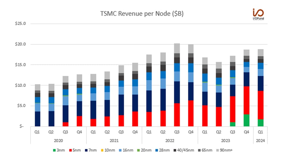
Revenue contribution from TSMC’s most advanced 3nm node dropped QoQ from 15% to 9% in Q1. Revenues fell nearly 40% QoQ from $2.9B to $1.7B in the most recent quarter. This is not necessarily unusual in the early ramp stages, given that the 5nm node saw a similar pattern in Q4 2020 and Q1 2021, where revenue contribution dipped before accelerating for multiple quarters. There is indication that TSMC will have to allocate more resources to 3nm, and this will come from 5nm fabrication equipment. Therefore, it may be in 2025 that we see 3nm exceed 20% percentage of revenue, which was forecast by management in a previous earnings call.
“We can convert one technology node capacity to the next one is because of our GI’s physical advantage, meaning, let me give you one example, our 3-nanometer and 5-nanometer are adjacent to each other, the fabs, and they are all connected. So it’s much easier for TSMC to convert from 5 to 3. And that doesn’t mean that every node can do the same.”“We can convert one technology node capacity to the next one is because of our GI’s physical advantage, meaning, let me give you one example, our 3-nanometer and 5-nanometer are adjacent to each other, the fabs, and they are all connected. So it’s much easier for TSMC to convert from 5 to 3. And that doesn’t mean that every node can do the same.”
In dollar terms, advanced nodes notched their two best quarters in Q4 and Q1, generating $13.2 billion and $12.3 billion, respectively. Q1’s soft 3nm sales were offset by sequential dollar gains in 5nm and 7nm, with advanced node revenue falling just 6.8% QoQ.
CEO C.C. Wei clarified in the earnings call that most of the current AI accelerators on the market “are in the 5- or 4-nanometer technology,” hence why we’re seeing strong 5nm sales and sequential growth in a seasonally slower quarter.
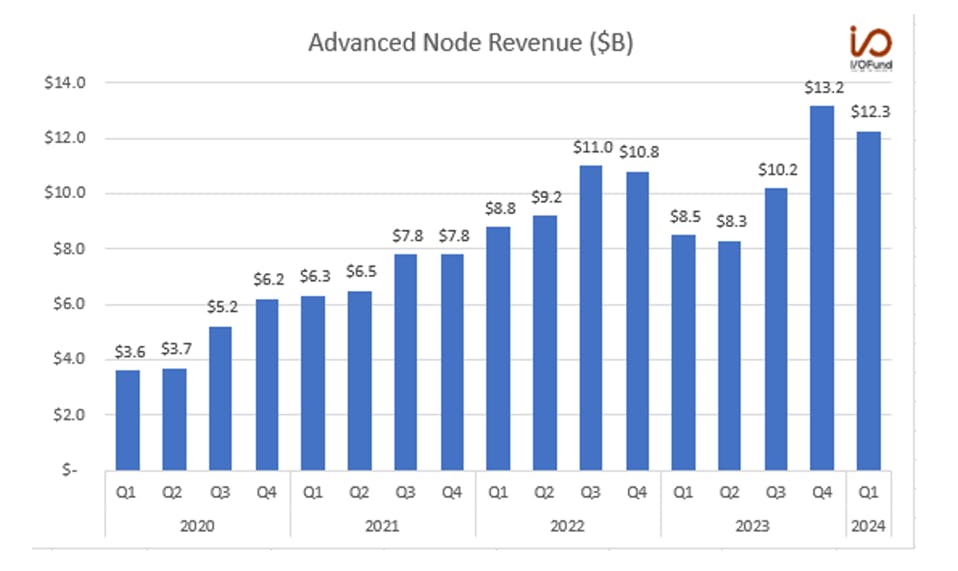
Despite most AI accelerators currently being produced on a 5nm node or 4NP node, including Nvidia’s upcoming Blackwell lineup, TSMC sees a clear path to increasing the 3nm node’s revenue contribution through the rest of the year. This will include converting 5nm node tools to support 3nm capacity and demand. Some of the capacity constraints are coming from HBM3e and the surge in CoWoS advanced packaging, which we’ve covered in more detail in our analysis: “Nvidia Q1 Earnings Preview: Blackwell and the $200 Billion Data Center.”